Thursday, June 21, 2012
Back to FPGA! Starting on FPGA Berzerk.
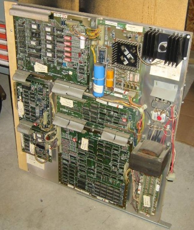
I managed to get my Berzerk board set back up and running just in time for the 2012 Northwest Pinball and Arcade Show. Berzerk is a particularly flaky board set due to a number of issues:
- Battery at the top of the whole board set that has a tendency to leak and cause acid damage.
- Tons of small boards with flaky interconnects.
- Bad power supply design.
This is what a Berzerk board set looks like:
Now that my Berzerk machine is working properly, I figure it's a good time to make some progress on learning about FPGA development. Berzerk is a good test case for this since I can implement a small board that is less complicated than a typical arcade board and test it in circuit with the real hardware. After all of the individual boards are implemented and tested in circuit with the real hardware, they can all be linked together inside of a single FPGA chip on a simple and much more reliable board.
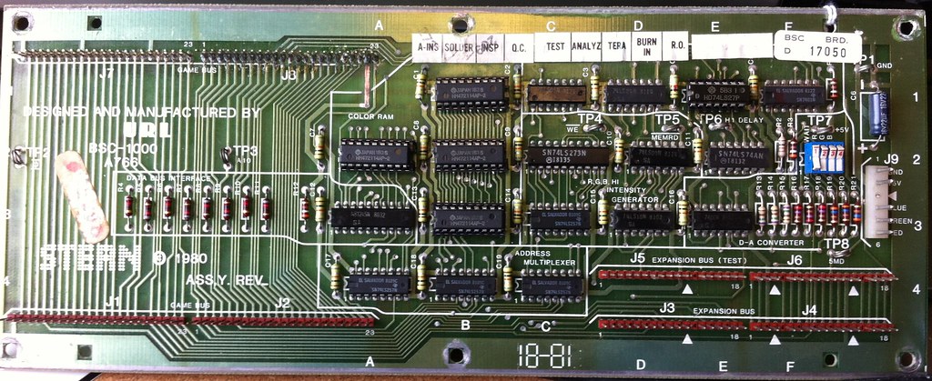
From what I've heard, Berzerk started off development as a black and white raster game. Close to the end of development, the team saw Galaxian, which is the first color arcade game made. They decided that in order to be competitive, they'd need to add color support to Berzerk. They did this by tacking on a dedicated board for dealing with color, which is the "Buffer System Color" board. In the pictures above, this is the wide/short board in the middle of the set. Here's the schematic for the BSC board:
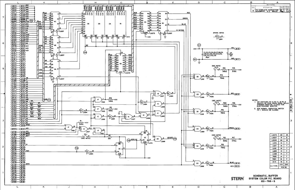
You can see the full resolution Berzerk schematics here: http://arcarc.xmission.com/PDF_Arcade_Manuals_and_Schematics/Berzerk.pdf
Now that I'm working in the same room as Jeri Ellsworth, it's really hard not to pick this stuff back up. She is super helpful when I can't figure stuff out. My friends Rick and Tanio plan on helping out with this too.
Since the BSC board is the simplest board in the set, I'm starting with it. Here's what the BSC board looks like:
The plan is to make a board that has all of the resistors that are near the boundary of the circuit.
- J1, J2, J7, and J8 data bus connectors as on the original BSC board.
- J3 and J4 expansion bus connectors for connecting to the original frame buffer board as on the original BSC board.
- 6-pin molex head for video output.
- Resistors on the right side of the schematic that make a simple 6-bit digital-to-analog (DAC) converter for video output. There are two bits for each of red, green, and blue.
- Resistors on the left side of the schematic on the data lines that are there to avoid reflections. (Jeri had to clue me on as to why these are there.)
- Something to convert from the 3.3V logic that is internal to the FPGA to the 5V logic on the original board set. Here's a discussion on how to do this with resistors: http://dbaspot.com/arch/381380-spartan-3e-intefacing-dummies.html. Via email, Jrok says "You can always buffer the 5v bus with something like a voltage level converter, the IDT quickswitch IDTQS3245 is a good example. Then you can run any 3.3v part and not have to worry about 5v tolerance on the FPGA side and use something like the Xilinx spartan 6 parts." I may go ahead and order some of those to be safe.
- Connectors to interface to the FX2 board and the LCD connector on the dev board.
The resistors in the middle of the schematic are just there as pull-ups. Will implement those internally in Verilog logic. I'll hard code the dipswitches to what is appropriate for the monitor that I'm using with my Berzerk for prototyping just the BSC board.
So far I have all the parts together to make an interface board. I've gone through a couple of tutorials to interface from Verilog and schematic capture to the I/O pins on the FPGA: Xilinx Verilog Tutorial and Xilinx Schematic Capture Tutorial.
Tuesday, February 9, 2010
Books about digital electronics and FPGA development that I like
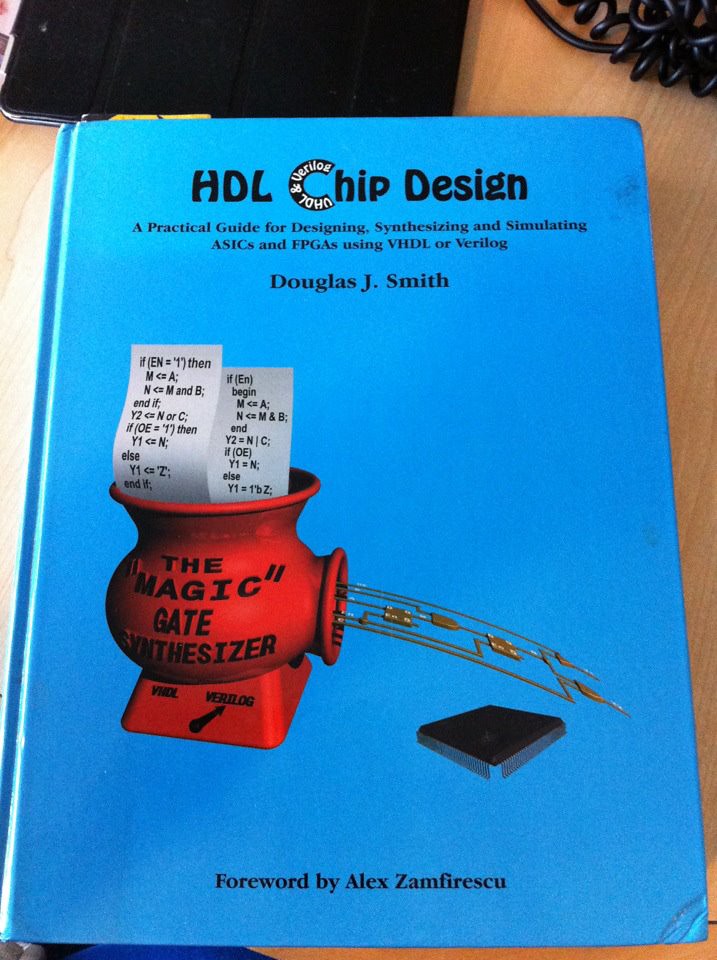
You end up coding in VHDL (or Verilog) for this stuff. This book is great for learning the language:
http://www.amazon.com/gp/aw/d.html/ref=redir_mdp_mobile/187-0765075-2752924?redirect=true&ref_=oss%5Fproduct&a=0262162245
This one is great if you are an electronics newb (like me) and want to learn enough to do FPGA programming:
http://www.amazon.com/gp/aw/d.html/ref=redir_mdp_mobile/187-0765075-2752924?redirect=true&ref_=oss%5Fproduct&a=0131733494
This last one is pretty expensive, but avoid the paperback version that is for sale on Amazon. It's a really poor printing (can't read a lot of the pages) that is made only for India and isn't supposed to be sold in the US.
Sunday, February 7, 2010
Pac-Man Logic Board Schematic Revision B
I scanned in the 3 pages and did the photoshop work for the pac-man logic board version b schematic. This is nice for panning around the whole schematic on your computer with no page breaks. This looks higher quality than most of the scans that I've seen out there, so I figured I'd share:
Pac-Man Logic Board Schematic Revision B
Pac-Man Logic Board Schematic Revision B
Saturday, January 23, 2010
Friday, January 22, 2010
color ROM 4a on the Pac-Man board
Every sprite (and I believe the background) in Pac-Man has at most 4 colors in it. Of the 4 colors, there is a 4-bit index into the palette ROM 7f mentioned in the previous post. Palette index 0 is transparent for sprites (and I assume black for the background?)

Here's the VHDL code for the ROM as generated by Mike J's romgen. Note that I've modified each x"00" through x"0f" value (4-bit palette index) to zero to avoid publishing the ROM data:

Here's the VHDL code for the ROM as generated by Mike J's romgen. Note that I've modified each x"00" through x"0f" value (4-bit palette index) to zero to avoid publishing the ROM data:
-- generated with romgen v3.0 by MikeJ
library ieee;
  use ieee.std_logic_1164.all;
  use ieee.std_logic_unsigned.all;
  use ieee.numeric_std.all;

library UNISIM;
  use UNISIM.Vcomponents.all;

entity PACROM_4A_DST is
  port (
    ADDR        : in    std_logic_vector(7 downto 0);
    DATA        : out   std_logic_vector(7 downto 0)
    );
end;

architecture RTL of PACROM_4A_DST is

  signal rom_addr : std_logic_vector(11 downto 0);

begin

  p_addr : process(ADDR)
  begin
     rom_addr <= (others => '0');
     rom_addr(7 downto 0) <= ADDR;
  end process;

  p_rom : process(rom_addr)
  begin
    DATA <= (others => '0');
    case rom_addr is
      when x"000" => DATA <= x"00";
      when x"001" => DATA <= x"00";
      when x"002" => DATA <= x"00";
      when x"003" => DATA <= x"00";
      when x"004" => DATA <= x"00";
      when x"005" => DATA <= x"00";
      when x"006" => DATA <= x"00";
      when x"007" => DATA <= x"00";
      when x"008" => DATA <= x"00";
      when x"009" => DATA <= x"00";
      when x"00A" => DATA <= x"00";
      when x"00B" => DATA <= x"00";
      when x"00C" => DATA <= x"00";

SNIP

      when x"0FC" => DATA <= x"00";
      when x"0FD" => DATA <= x"00";
      when x"0FE" => DATA <= x"00";
      when x"0FF" => DATA <= x"00";
      when others => DATA <= (others => '0');
    end case;
  end process;
end RTL;
Subscribe to:
Comments (Atom)